Sunday, 25 November 2012

Superconducting Amplifier Designed to Study the Universe


Superconducting Amplifier Designed to Study the Universe

July 18, 2012
New Amp to Study the Universe
The new amplifier consists of a superconducting material (niobium titanium nitride) coiled into a double spiral 16 millimeters in diameter. Image credit: NASA/JPL-Caltech
Designed by scientists at the California Institute of Technology and at NASA’s Jet Propulsion Laboratory, a new amplifier using titanium nitride and niobium titanium nitride will help researchers study the universe.
Researchers at NASA’s Jet Propulsion Laboratory and the California Institute of Technology, both in Pasadena, have developed a new type of amplifier for boosting electrical signals. The device can be used for everything from studying stars, galaxies and black holes to exploring the quantum world and developing quantum computers.
“This amplifier will redefine what it is possible to measure,” said Jonas Zmuidzinas, chief technologist at JPL, who is Caltech’s Merle Kingsley Professor of Physics and a member of the research team.
An amplifier is a device that increases the strength of a weak signal. “Amplifiers play a basic role in a wide range of scientific measurements and in electronics in general,” said Peter Day, a principal scientist at JPL and a visiting associate in physics at Caltech. “For many tasks, current amplifiers are good enough. But for the most demanding applications, the shortcomings of the available technologies limit us.”
One of the key features of the new amplifier is that it incorporates superconductors-materials that allow an electric current to flow with zero resistance when lowered to certain temperatures. For their amplifier, the researchers are using titanium nitride and niobium titanium nitride, which have just the right properties to allow the pump signal to amplify the weak signal.
Although the amplifier has a host of potential applications, the reason the researchers built the device was to help them study the universe. The team built the instrument to boost microwave signals, but the new design can be used to build amplifiers that help astronomers observe in a wide range of wavelengths, from radio waves to X-rays.
“It’s hard to predict what all of the applications are going to end up being, but a nearly perfect amplifier is a pretty handy thing to have in your bag of tricks,” Zmuidzinas said. And by creating their new device, the researchers have shown that it is indeed possible to build an essentially perfect amplifier. “Our instrument still has a few rough edges that need polishing before we would call it perfect, but we think our results so far show that we can get there.”
In addition to Zmuidzinas and Day, the other authors of the paper are Byeong Ho Eom of Caltech, and Henry LeDuc of JPL. This research was supported by NASA, the Keck Institute for Space Studies, and the JPL Research and Technology Development program. JPL is managed by Caltech for NASA.
Source: Priscilla Vega, Jet Propulsion Laboratory
Image: NASA/JPL-Caltech

Macroporous Silicon and Pyrolyzed Polyacrylonitrile form High Performance Anodes


Macroporous Silicon and Pyrolyzed Polyacrylonitrile form High Performance Anodes

July 18, 2012
pores in silicon give the material room to expand when soaking in lithium ions in a rechargeable battery
Micronwide pores in silicon give the material room to expand when soaking in lithium ions in a rechargeable battery, according to researchers at Rice University and Lockheed Martin. The scientists are developing the material to replace graphite as the anode in common batteries for commercial electronics and perhaps even electric vehicles. (Credit: Madhuri Thakur/Rice University)
By detaching a freestanding macroporous silicon film from the underlying bulk silicon and combining it with pyrolyzed polyacrylonitrile, researchers have found a way to make multiple high-performance anodes from a single silicon wafer.
Researchers at Rice University and Lockheed Martin reported this month that they’ve found a way to make multiple high-performance anodes from a single silicon wafer. The process uses simple silicon to replace graphite as an element in rechargeable lithium-ion batteries, laying the groundwork for longer-lasting, more powerful batteries for such applications as commercial electronics and electric vehicles.
The work led by Sibani Lisa Biswal, an assistant professor of chemical and biomolecular engineering at Rice, and lead author Madhuri Thakur, a Rice research scientist, details the process by which Swiss cheese-like silicon “sponges” that store more than four times their weight in lithium can be electrochemically lifted off of wafers.
Silicon – one of the most common elements on Earth – is a candidate to replace graphite as the anode in batteries. In a previous advance by Biswal and her team, porous silicon was found to soak up 10 times more lithium than graphite.
Because silicon expands as it absorbs lithium ions, the sponge-like configuration gives it room to grow internally without degrading the battery’s performance, the researchers reported. The promise that silicon sponges, with pores a micron wide and 12 microns deep, held for batteries was revealed in 2010 at Rice’s Buckyball Discovery Conference by Thakur, Biswal, their Rice colleague Michael Wong, a professor of chemical and biomolecular engineering and of chemistry, and Steven Sinsabaugh, a Lockheed Martin Fellow. But even then Thakur saw room for improvement as the solid silicon substrate served no purpose in absorbing lithium.
silicon sponge
A Swiss cheese-like silicon sponge lifts off from a wafer in a process developed by researchers at Rice University and Lockheed Martin who hope to replace graphite anodes in lithium-ion batteries with a material that has a larger capacity for lithium. (Credit: Madhuri Thakur/Rice University)
In the new work, they discovered the electrochemical etching process used to create the pores can also separate the sponge from the substrate, which is then reused to make more sponges. The team noted that at least four films can be drawn from a standard 250-micron-thick wafer. Removing the sponge from the silicon substrate also eliminates a limiting factor to the amount of lithium that can be stored.
The team also found a way to make the pores 50 microns deep. Once lifted from the wafer, the sponges, now open at the top and bottom, were enhanced for conductivity by soaking them in a conductive polymer binder, pyrolyzed polyacrylonitrile (PAN).
The product was a tough film that could be attached to a current collector (in this case, a thin layer of titanium on copper) and placed in a battery configuration. The result was a working lithium-ion battery with a discharge capacity of 1,260 milliamp-hours per gram, a capability that should lead to batteries that last longer between charges.
silicon sponges may make tenacious batteries
A sponge formed from a solid wafer of silicon helps the material realize its potential to hold 10 times the amount of lithium ions than current materials used in rechargeable batteries. The material was developed by Rice University and Lockheed Martin. (Credit: Madhuri Thakur/Rice University)
The researchers compared batteries using their film before and after the PAN-and-bake treatment. Before, the batteries started with a discharge capacity of 757 milliamp-hours per gram, dropped rapidly after the second charge-discharge cycle and failed completely by cycle 15. The treated film increased in discharge capacity over the first four cycles – typical for porous silicon, the researchers said – and the capacity remained consistent through 20 cycles.
The researchers are investigating techniques that promise to vastly increase the number of charge-discharge cycles, a critical feature for commercial applications in which rechargeable batteries are expected to last for years.
Co-authors of the paper are postdoctoral researcher Roderick Pernites, alumnus Naoki Nitta and Lockheed Martin researcher Mark Isaacson.
The work was supported by the Lockheed Martin Advanced Nanotechnology Center of Excellence at Rice.
Source: Mike Williams, Rice University News
Images: Madhuri Thakur/Rice University

Self-Assembling Polymer Molecules Create Complex Microchip Structures


Self-Assembling Polymer Molecules Create Complex Microchip Structures

July 19, 2012
Chips with self-assembling rectangles
An artist’s representation of the structures produced by this self-assembly method shows a top-down view, with the posts produced by electron-beam lithography shown in blue, and the resulting self-assembled shapes shown in white. Image: Yan Liang
Using tiny posts to guide the patterning of self-assembling polymer molecules, researchers at MIT developed a new technique to create perfect square and rectangular patterns of tiny polymer wires on microchips.
Researchers at MIT have developed a new approach to creating the complex array of wires and connections on microchips, using a system of self-assembling polymers. The work could eventually lead to a way of making more densely packed components on memory chips and other devices.
The new method — developed by MIT visiting doctoral student Amir Tavakkoli of the National University of Singapore, along with two other graduate students and three professors in MIT’s departments of Electrical Engineering and Computer Science (EECS) and Materials Science and Engineering (DMSE) — is described in a paper published in the journal Advanced Materials.
The process is closely related to a method the same team described last month in a paper in Science, which makes it possible to produce three-dimensional configurations of wires and connections using a similar system of self-assembling polymers.
In the new paper, the researchers describe a system for producing arrays of wires that meet at right angles, forming squares and rectangles. While these shapes are the basis for most microchip circuit layouts, they are quite difficult to produce through self-assembly. When molecules self-assemble, explains Caroline Ross, the Toyota Professor of Materials Science and Engineering and a co-author of the papers, they have a natural tendency to create hexagonal shapes — as in a honeycomb or an array of soap bubbles between sheets of glass.
For example, an array of tiny ball bearings in a box “tends to give a hexagonal symmetry, even though it’s in a square box,” Ross says. “But that’s not what circuit designers want. They want patterns with 90-degree angles” — so overcoming that natural tendency was essential to producing a useful self-assembling system, she says.
The team’s solution creates an array of tiny posts on the surface that guides the patterning of the self-assembling polymer molecules. This turns out to have other advantages as well: In addition to producing perfect square and rectangular patterns of tiny polymer wires, the system also enables the creation of a variety of shapes of the material itself, including cylinders, spheres, ellipsoids and double cylinders. “You can generate this astounding array of features,” Ross says, “with a very simple template.”
Karl Berggren, an associate professor of electrical engineering at MIT and a co-author of the paper, explains that these complex shapes are possible because “the template, which is coated so as to repel one of the polymer components, causes a lot of local strain on the pattern. The polymer then twists and turns to try to avoid this strain, and in so doing rearranges on the surface. So we can defeat the polymer’s natural inclinations, and make it create much more interesting patterns.”
This system can also produce features, such as arrays of holes in the material, whose spacing is much closer than what can be achieved using conventional chip-making methods. That means it can produce much more closely packed features on the chip than today’s methods can create — an important step in the ongoing efforts to pack more and more electronic components onto a given microchip.
“This new technique can produce multiple [shapes or patterns] simultaneously,” Tavakkoli says. It can also make “complex patterns, which is an objective for nanodevice fabrication,” with fewer steps than current processes. Fabricating a large area of complex circuitry on a chip using electron-beam lithography “could take several months,” he says. By contrast, using the self-assembling polymer method would take only a few days.
That’s still far too long for manufacturing a commercial product, but Ross explains that this step needs to be done only once to create a master pattern, which can then be used to stamp a coating on other chips in a very rapid fabrication process.
The technique could extend beyond microchip fabrication as well, Ross says. For example, one approach to the quest to pack ever-greater amounts of data onto magnetic media such as computer hard disks is to use a magnetic coating with a very fine pattern stamped into it, precisely defining the areas where each bit of data is to be stored. Such fine patterning could potentially be created using this self-assembly method, she says, and then stamped onto the disks.
Craig Hawker, a professor of chemistry and biochemistry at the University of California at Santa Barbara who was not involved in this work, says, “There is a growing need and requirement for industry to find an alternative to traditional photolithography for the fabrication of cutting-edge microelectronic devices. This work represents a pivotal achievement in this area and clearly demonstrates that structures once considered impossible to achieve by a self-assembly strategy can now be prepared with a high degree of fidelity.”
Tavakkoli and Ross’ colleagues in this work are DMSE doctoral students Adam Hannon and Kevin Gotrik, DMSE professor Alfredo Alexander-Katz and EECS professor Karl Berggren. The research, which included work at MIT’s Nanostructures Laboratory and Scanning-Electron-Beam Lithography facility, was funded by the Semiconductor Research Corporation, the Center on Functional Engineered Nano Architectonics, the National Resources Institute, the Singapore-MIT Alliance, the National Science Foundation, the Taiwan Semiconductor Manufacturing Company and Tokyo Electron.
Source: David L. Chandler, MIT News Office
Image: Yan Liang

Engineers to Develop a Smart Suit That Improves Physical Endurance


Engineers to Develop a Smart Suit That Improves Physical Endurance

July 20, 2012
Smart suit improves human physical endurance
The new wearable system would be made from soft, stretchable, assistive devices, which would help improve physical endurance for soldiers in the field. Courtesy of the Wyss Institute
Engineers at the Wyss Institute are working on a smart suit that helps improve physical endurance for soldiers in the field, delaying the onset of fatigue and potentially improving the body’s resistance to injuries when carrying heavy loads.
The Wyss Institute for Biologically Inspired Engineering at Harvard University today announced that it has received a $2.6 million contract from the Defense Advanced Research Projects Agency (DARPA) to develop a smart suit that helps improve physical endurance for soldiers in the field.
The novel wearable system would potentially delay the onset of fatigue, enabling soldiers to walk longer distances, and also potentially improve the body’s resistance to injuries when carrying heavy loads.
Lightweight, efficient, and nonrestrictive, the proposed suit will be made from soft wearable assistive devices that integrate several novel Wyss technologies. One is a stretchable sensor that would monitor the body’s biomechanics without the need for the typical rigid components that often interfere with motion. The system could potentially detect the onset of fatigue. Additionally, one of the technologies in the suit may help the wearer maintain balance by providing low-level mechanical vibrations that boost the body’s sensory functions.
The new smart suit will be designed to overcome several of the problems typically associated with current wearable systems, including their large power requirements and rigid overall structures, which restrict normal movement and can be uncomfortable.
Although the DARPA project is focused on assisting and protecting soldiers in the field, the technologies being developed could have many other applications as well. For instance, similar soft-wearable devices hold the potential to increase endurance in the elderly and help improve mobility for people with physical disabilities.
Conor Walsh, assistant professor of mechanical and biomedical engineering at the Harvard School of Engineering and Applied Sciences (SEAS) and Wyss core faculty member, will lead this interdisciplinary program. The program will include collaborations with core faculty member Rob Wood and Wyss Technology Development Fellow Yong-Lae Park, for developing soft sensor technologies, and with core faculty member George Whitesides, for developing novel soft interfaces between the device and the wearer. Wood is also the Gordon McKay Professor of Electrical Engineering at the SEAS, and Whitesides is also the Woodford L. and Ann A. Flowers University Professor at Harvard. Sang-bae Kim, assistant professor of mechanical engineering at the Massachusetts Institute of Technology, and Ken Holt, associate professor at Boston University’s College of Health and Rehabilitation Sciences, will also play key roles on the project.
Also working on the project will be several members of the Wyss Advanced Technology Team who will oversee the testing of prototypes in the Wyss Institute’s biomechanics lab, using motion-capture capabilities that can measure the impact of the suit on specific muscles and joints.
“This project is a excellent example of how Wyss researchers from different disciplines work side by side with experts in product development to develop solutions to difficult problems that might not otherwise be possible,” said Donald Ingber, Wyss founding director and the Judah Folkman Professor of Vascular Biology in the Department of Pathology.
Source: Twig Mowatt, Wyss Institute Communications; Harvard Gazette
Image: Wyss Institute

Highly Transparent Polymer Solar Cell Produces Energy by Absorbing Near-Infrared Light


Highly Transparent Polymer Solar Cell Produces Energy by Absorbing Near-Infrared Light

July 20, 2012
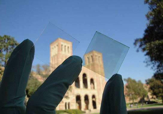
transparent solar cells for windows
Visibly Transparent Polymer Solar Cells Produced by Solution Processing.
Using a photoactive plastic that converts infrared light into an electrical current, scientists developed a new kind of polymer solar cell that produces energy by absorbing mainly near-infrared light, not visible light, making the cells nearly 70% transparent to the human eye.
UCLA researchers have developed a new transparent solar cell that is an advance toward giving windows in homes and other buildings the ability to generate electricity while still allowing people to see outside. Their study appears in the journal ACS Nano.
The UCLA team describes a new kind of polymer solar cell (PSC) that produces energy by absorbing mainly infrared light, not visible light, making the cells nearly 70% transparent to the human eye. They made the device from a photoactive plastic that converts infrared light into an electrical current.
“These results open the potential for visibly transparent polymer solar cells as add-on components of portable electronics, smart windows and building-integrated photovoltaics and in other applications,” said study leader Yang Yang, a UCLA professor of materials science and engineering, who also is director of the Nano Renewable Energy Center at California NanoSystems Institute (CNSI).
Yang added that there has been intense world-wide interest in so-called polymer solar cells. “Our new PSCs are made from plastic-like materials and are lightweight and flexible,” he said. “More importantly, they can be produced in high volume at low cost.”
Polymer solar cells have attracted great attention due to their advantages over competing solar cell technologies. Scientists have also been intensely investigating PSCs for their potential in making unique advances for broader applications. Several such applications would be enabled by high-performance visibly transparent photovoltaic (PV) devices, including building-integrated photovoltaics and integrated PV chargers for portable electronics.
Previously, many attempts have been made toward demonstrating visibly transparent or semitransparent PSCs. However, these demonstrations often result in low visible light transparency and/or low device efficiency because suitable polymeric PV materials and efficient transparent conductors were not well deployed in device design and fabrication.
A team of UCLA researchers from the California NanoSystems Institute, the UCLA Henry Samueli School of Engineering and Applied Science and UCLA’s Department of Chemistry and Biochemistry have demonstrated high-performance, solution-processed, visibly transparent polymer solar cells through the incorporation of near-infrared light-sensitive polymer and using silver nanowire composite films as the top transparent electrode. The near-infrared photoactive polymer absorbs more near-infrared light but is less sensitive to visible light, balancing solar cell performance and transparency in the visible wavelength region.
Another breakthrough is the transparent conductor made of a mixture of silver nanowire and titanium dioxide nanoparticles, which was able to replace the opaque metal electrode used in the past. This composite electrode also allows the solar cells to be fabricated economically by solution processing. With this combination, 4% power-conversion efficiency for solution-processed and visibly transparent polymer solar cells has been achieved.
“We are excited by this new invention on transparent solar cells, which applied our recent advances in transparent conducting windows (also published in ACS Nano) to fabricate these devices,” said Paul S.Weiss, CNSI director and Fred Kavli Chair in NanoSystems Sciences.
Study authors also include Weiss; materials science and engineering postdoctoral researcher Rui Zhu; Ph.D. candidates Chun-Chao Chen, Letian Dou, Choong-Heui Chung, Tze-Bin Song and Steve Hawks; Gang Li, who is former vice president of engineering for Solarmer Energy, Inc., a startup from UCLA; and CNSI postdoctoral researcher Yue Bing Zheng.
The study was supported by the Henry Samueli School of Engineering and Applied Science, the Office of Naval Research, and The Kavli Foundation.
Source: Jennifer Marcus, UCLA Newsroom
Image: UCLA Newsroom

Nanotechnology Used to Create “Magnetic Domain-Wall Ratchet” Memory


Nanotechnology Used to Create “Magnetic Domain-Wall Ratchet” Memory

July 23, 2012
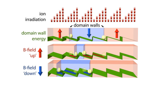
computer memory that is built up from moving bits of magnetized areas
Ion irradiation creates an asymmetric potential or ‘ratchet’ for the main walls (visualized as light-yellow spheres). The bit with a magnetic coating is shifted one position to the left by sequentially positioning a field upwards and downwards.
A newly published study details how scientists at the Eindhoven University of Technology developed “magnetic domain-wall ratchet” memory, computer memory that is built up from moving bits of magnetized areas.
Researchers from TU/e and the FOM Foundation have successfully made a ‘magnetic domain-wall ratchet’ memory, a computer memory that is built up from moving bits of magnetized areas. This memory potentially offers many advantages compared to standard hard disks, such as a higher speed, lower electricity consumption and much longer life. Using concentrated ion bundles the researchers have influenced the magnetic wires the bits move through, and they have successfully controlled bits at the nanometer scale and subsequently constructed a new memory. The research results were published online by Nature Nanotechnology on Sunday 15 July.
The bits in a nanowire can be conceptualized as areas that can have two possible magnetic directions, a 0 or a 1. Usually all of the bits are simultaneously set at either 0 or 1 during the construction as they reverse like compass needles. The researchers have now demonstrated that bits can be coherently transferred without the information they contain being lost. This method of magnetic data transport is radically different from that in current computers, where rotating magnetic disks are mechanically moved to address data.
Saw tooth
By cleverly varying how the ions are fired across a nanowire, a repeating, saw-tooth-shaped energy landscape is created. This asymmetric saw tooth is crucial: it forces a domain wall, the boundary between bits, to move in a single direction under a variable magnetic field. Due to the variable magnetic field the force on the domain wall continually reverses and this is alternately pushed over the incline and then subsequently pushed back against the sharp edge (see Figure). After one cycle of the magnetic field two domain walls are pushed up by exactly one position. This net transfer of a bit would be impossible without saw-tooth potential.
The researchers used a circular magnetic wire. By using this circle the domain walls can always rotate and the bits are retained. This one-way traffic of the domains is a movement comparable to that of a rattle or ‘ratchet’.
Unique opportunities
The discovery offers unique opportunities for the development of alternative memory concepts. After the proof-of-principle experiments the scientists will focus on a next generation ratchet. This will be based on radical new effects such as the use of spin currents generated in the neighboring non-magnetic layers or the use of electric fields to influence the domain or movement.
Source: Eindhoven University of Technology
Image: Eindhoven University of Technology

Microorganisms Convert Renewable Electricity into Carbon-Neutral Methane


Microorganisms Convert Renewable Electricity into Carbon-Neutral Methane

July 25, 2012
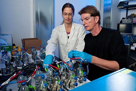
using microbes that can convert renewable electricity into carbon-neutral methane
Post-doctoral fellow Svenja Lohner, left, and Professor Alfred Spormann. Their research, along with the work of others, could help solve one of the biggest challenges for large-scale renewable energy: What to do with surplus electricity generated by photovoltaic power stations and wind farms. L.A. Cicero
Taking a “greener” approach to methane production, scientists from Stanford and Pennsylvania State are raising colonies of microorganisms, called methanogens, which have the ability to turn electrical energy into pure methane in microbial process that is carbon neutral.
Microbes that convert electricity into methane gas could become an important source of renewable energy, according to scientists from Stanford and Pennsylvania State universities.
Researchers at both campuses are raising colonies of microorganisms, called methanogens, which have the remarkable ability to turn electrical energy into pure methane – the key ingredient in natural gas. The scientists’ goal is to create large microbial factories that will transform clean electricity from solar, wind or nuclear power into renewable methane fuel and other valuable chemical compounds for industry.
“Most of today’s methane is derived from natural gas, a fossil fuel,” said Alfred Spormann, a professor of chemical engineering and of civil and environmental engineering at Stanford. “And many important organic molecules used in industry are made from petroleum. Our microbial approach would eliminate the need for using these fossil resources.”
Stanford Professor Alfred Spormann explains how the system works.
While methane itself is a formidable greenhouse gas, 20 times more potent than CO2, the microbial methane would be safely captured and stored, thus minimizing leakage into the atmosphere, Spormann said.
“The whole microbial process is carbon neutral,” he explained. “All of the CO2 released during combustion is derived from the atmosphere, and all of the electrical energy comes from renewables or nuclear power, which are also CO2-free.”
Methane-producing microbes, he added, could help solve one of the biggest challenges for large-scale renewable energy: What to do with surplus electricity generated by photovoltaic power stations and wind farms.
“Right now there is no good way to store electricity,” Spormann said. “However, we know that some methanogens can produce methane directly from an electrical current. In other words, they metabolize electrical energy into chemical energy in the form of methane, which can be stored. Understanding how this metabolic process works is the focus of our research. If we can engineer methanogens to produce methane at scale, it will be a game changer.”
‘Green’ methane
Burning natural gas accelerates global warming by releasing carbon dioxide that’s been trapped underground for millennia. The Stanford and Penn State team is taking a “greener” approach to methane production. Instead of drilling rigs and pumps, the scientists envision large bioreactors filled with methanogens – single-cell organisms that resemble bacteria but belong to a genetically distinct group of microbes called archaea.
By human standards, a methanogen’s lifestyle is extreme. It cannot grow in the presence of oxygen. Instead, it regularly dines on atmospheric carbon dioxideand electrons borrowed from hydrogen gas. The byproduct of this microbial meal is pure methane, which methanogens excrete into the atmosphere.
The researchers plan to use this methane to fuel airplanes, ships and vehicles. In the ideal scenario, cultures of methanogens would be fed a constant supply of electrons generated from emissions-free power sources, such as solar cells, wind turbines and nuclear reactors. The microbes would use these clean electrons to metabolize carbon dioxide into methane, which can then be stockpiled and distributed via existing natural gas facilities and pipelines when needed.
When the microbial methane is burnt as fuel, carbon dioxide would be recycled back into the atmosphere where it originated from – unlike conventional natural gas combustion, which contributes to global warming.
“Microbial methane is much more ecofriendly than ethanol and other biofuels,” Spormann said. “Corn ethanol, for example, requires acres of cropland, as well as fertilizers, pesticides, irrigation and fermentation. Methanogens are much more efficient, because they metabolize methane in just a few quick steps.”
Microbial communities
For this new technology to become commercially viable, a number of fundamental challenges must be addressed.
“While conceptually simple, there are significant hurdles to overcome before electricity-to-methane technology can be deployed at a large scale,” said Bruce Logan, a professor of civil and environmental engineering at Penn State. “That’s because the underlying science of how these organisms convert electrons into chemical energy is poorly understood.”
In 2009, Logan’s lab was the first to demonstrate that a methanogen strain known as Methanobacterium palustre could convert an electrical current directly into methane. For the experiment, Logan and his Penn State colleagues built a reverse battery with positive and negative electrodes placed in a beaker of nutrient-enriched water.
The researchers spread a biofilm mixture of M. palustre and other microbial species onto the cathode. When an electrical current was applied, the M. palustre began churning out methane gas.
“The microbes were about 80 percent efficient in converting electricity to methane,” Logan said.
The rate of methane production remained high as long as the mixed microbial community was intact. But when a previously isolated strain of pure M. palustre was placed on the cathode alone, the rate plummeted, suggesting that methanogens separated from other microbial species are less efficient than those living in a natural community.
“Microbial communities are complex,” Spormann added. “For example, oxygen-consuming bacteria can help stabilize the community by preventing the build-up of oxygen gas, which methanogens cannot tolerate. Other microbes compete with methanogens for electrons. We want to identify the composition of different communities and see how they evolve together over time.”
Microbial zoo
To accomplish that goal, Spormann has been feeding electricity to laboratory cultures consisting of mixed strains of archaea and bacteria. This microbial zoo includes bacterial species that compete with methanogens for carbon dioxide, which the bacteria use to make acetate – an important ingredient in vinegar, textiles and a variety of industrial chemicals.
“There might be organisms that are perfect for making acetate or methane but haven’t been identified yet,” Spormann said. “We need to tap into the unknown, novel organisms that are out there.”
At Penn State, Logan’s lab is designing and testing advanced cathode technologies that will encourage the growth of methanogens and maximize methane production. The Penn State team is also studying new materials for electrodes, including a carbon-mesh fabric that could eliminate the need for platinum and other precious metal catalysts.
“Many of these materials have only been studied in bacterial systems but not in communities with methanogens or other archaea,” Logan said. “Our ultimate goal is to create a cost-effective system that reliably and robustly produces methane from clean electrical energy. It’s high-risk, high-reward research, but new approaches are needed for energy storage and for making useful organic molecules without fossil fuels.”
The Stanford-Penn State research effort is funded by a three-year grant from the Global Climate and Energy Project at Stanford.
Source: Mark Shwartz, Stanford University News
Image: L.A. Cicero


New Class of Synthetic Vaccines Piggyback on 3-D DNA Nanostructures


New Class of Synthetic Vaccines Piggyback on 3-D DNA Nanostructures

July 25, 2012
DNA nanostructures to make safer and more effective vaccines
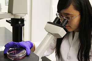
Xiaowei Liu examines cells to test whether DNA nanostructures could reside comfortably within the appropriate compartment of the cells and be stable for several hours—-long enough to set in motion an immune cascade.
Scientists at the Biodesign Institute at Arizona State University are using DNA nanotechnology to make an entirely new class of synthetic vaccines that could be delivered by piggybacking onto self-assembled, three-dimensional DNA nanostructures.
In a quest to make safer and more effective vaccines, scientists at the Biodesign Institute at Arizona State University have turned to a promising field called DNA nanotechnology to make an entirely new class of synthetic vaccines.
In a study published in the journal Nano Letters, Biodesign immunologist Yung Chang joined forces with her colleagues, including DNA nanotechnology innovator Hao Yan, to develop the first vaccine complex that could be delivered safely and effectively by piggybacking onto self-assembled, three-dimensional DNA nanostructures.
“When Hao treated DNA not as a genetic material, but as a scaffolding material, that made me think of possible applications in immunology,” said Chang, an associate professor in the School of Life Sciences and a researcher in the Biodesign Institute’s Center for Infectious Diseases and Vaccinology. “This provided a great opportunity to try to use these DNA scaffolds to make a synthetic vaccine.”
“The major concern was: Is it safe? We wanted to mimic the assembly of molecules that can trigger a safe and powerful immune response in the body. As Hao’s team has developed a variety of interesting DNA nanostructures during the past few years, we have been collaborating more and more with a goal to further explore some promising human health applications of this technology.”
The core multidisciplinary research team members also included: ASU chemistry and biochemistry graduate student and paper first author Xiaowei Liu, visiting professor Yang Xu, chemistry and biochemistry assistant professor Yan Liu, School of Life Sciences undergraduate Craig Clifford and Tao Yu, visiting graduate student from Sichuan University.
Chang points out that vaccines have led to the some of the most effective public health triumphs in all of medicine. The state-of-the-art in vaccine development relies on genetic engineering to assemble immune system stimulating proteins into virus-like particles (VLPs) that mimic the structure of natural viruses—minus the harmful genetic components that cause disease.
DNA nanotechnology, where the molecule of life can be assembled into 2-D and 3-D shapes, has an advantage of being a programmable system that can precisely organize molecules to mimic the actions of natural molecules in the body.
“We wanted to test several different sizes and shapes of DNA nanostructures and attach molecules to them to see if they could trigger an immune response,” said Yan, the Milton D. Glick Distinguished Chair in the Department of Chemistry and Biochemistry and researcher in Biodesign’s Center for Single Molecule Biophysics. With their biomimicry approach, the vaccine complexes they tested closely resembled natural viral particles in size and shape.
As proof of concept, they tethered onto separate pyramid-shaped and branched DNA structures a model immune stimulating protein called streptavidin (STV) and immune response boosting compound called an adjuvant (CpG oligo-deoxynucletides) to make their synthetic vaccine complexes.
First, the group had to prove that the target cells could gobble the nanostructures up. By attaching a light-emitting tracer molecule to the nanostructures, they found the nanostructures residing comfortably within the appropriate compartment of the cells and stable for several hours—-long enough to set in motion an immune cascade.
Next, in a mouse challenge, they targeted the delivery of their vaccine cargo to cells that are first responders in initiating an effective immune response, coordinating interaction of important components, such as: antigen presenting cells, including macrophages, dendritic cells and B cells. After the cargo is internalized in the cell, they are processed and “displayed” on the cell surface to T cells, white blood cells that play a central role in triggering a protective immune response. The T cells, in turn, assist B cells with producing antibodies against a target antigen.
To properly test all variables, they injected: 1) the full vaccine complex 2) STV (antigen) alone 3) the CpG (adjuvant) mixed with STV.
Over the course of 70 days, the group found that mice immunized with the full vaccine complex developed a more robust immune response up to 9-fold higher than the CpG mixed with STV. The pyramid (tetrahedral) shaped structure generated the greatest immune response. Not only was immune response to the vaccine complex specific and effective, but also safe, as the research team showed, using two independent methods, that no immune response triggered from introducing the DNA platform alone.
“We were very pleased,” said Chang. “It was so nice to see the results as we predicted. Many times in biology we don’t see that.”
With the ability to target specific immune cells to generate a response, the team is excited about the prospects of this new platform. They envision applications where they could develop vaccines that require multiple components, or customize their targets to tailor the immune response.
Furthermore, there is the potential to develop targeted therapeutics in a similar manner as some of the new generation of cancer drugs.
Overall, though the field of DNA is still young, the research is advancing at a breakneck pace toward translational science that is making an impact on health care, electronics, and other applications.
While Chang and Yan agree that there is still much room to explore the manipulation and optimization of the nanotechnology, it also holds great promise. “With this proof of concept, the range of antigens that we could use for synthetic vaccine develop is really unlimited,” said Chang.
The work was supported by funding from the Department of Defense and National Institutes of Health (National Cancer Institute, National Institute of Drug Abuse).
Source: ASU Biodesign Institute
Image: ASU Biodesign Institute

NASA’s Space Launch System Passes Review, Moving to Preliminary Design Phase


NASA’s Space Launch System Passes Review, Moving to Preliminary Design Phase

July 26, 2012
NASA's Space Launch System
SLS Architecture Reference Configuration
An artist rendering of the various configurations of NASA’s Space Launch System (SLS), managed by the Marshall Space Flight Center in Huntsville, Ala. The flexible configuration, sharing the same basic core-stage, allows for different crew and cargo flights as needed, promoting efficiency, time and cost savings. The SLS enables exploration missions beyond low-Earth orbit and support travel to asteroids, Mars and other destinations within our solar system. Image credit: NASA
With the hope of bringing explorers to nearby asteroids, Mars and its moons, and to destinations even farther across our solar system, NASA’s Space Launch System passed several major agency reviews and is now moving to its preliminary design phase.
The rocket that will launch humans farther into space than ever before passed a major NASA review Wednesday. The Space Launch System (SLS) Program completed a combined System Requirements Review and System Definition Review, which set requirements of the overall launch vehicle system. SLS now moves ahead to its preliminary design phase.
The SLS will launch NASA’s Orion spacecraft and other payloads, and provide an entirely new capability for human exploration beyond low Earth orbit.
These NASA reviews set technical, performance, cost and schedule requirements to provide on-time development of the heavy-lift rocket. As part of the process, an independent review board comprised of technical experts from across NASA evaluated SLS Program documents describing vehicle specifications, budget and schedule. The board confirmed SLS is ready to move from concept development to preliminary design.
expanded view of an artist rendering of the 70-metric-ton configuration of NASA's Space Launch System
An expanded view of an artist rendering of the 70-metric-ton configuration of NASA’s Space Launch System. (NASA)
“This new heavy-lift launch vehicle will make it possible for explorers to reach beyond our current limits, to nearby asteroids, Mars and its moons, and to destinations even farther across our solar system,” said William Gerstenmaier, associate administrator for the Human Exploration and Operations Mission Directorate at NASA Headquarters in Washington. “The in-depth assessment confirmed the basic vehicle concepts of the SLS, allowing the team to move forward and start more detailed engineering design.”
The reviews also confirmed the SLS system architecture and integration with the Orion spacecraft, managed by NASA’s Johnson Space Center in Houston, and the Ground Systems Development and Operations Program, which manage the operations and launch facilities at NASA’s Kennedy Space Center in Florida.
“This is a pivotal moment for this program and for NASA,” said SLS Program Manager Todd May. “This has been a whirlwind experience from a design standpoint. Reaching this key development point in such a short period of time, while following the strict protocol and design standards set by NASA for human spaceflight is a testament to the team’s commitment to delivering the nation’s next heavy-lift launch vehicle.”
expanded view of an artist rendering of the 130 metric ton configuration of NASA's Space Launch System
An expanded view of an artist rendering of the 130 metric ton configuration of NASA’s Space Launch System. (NASA)
SLS reached this major milestone less than 10 months after the program’s inception. The combination of the two assessments represents a fundamentally different way of conducting NASA program reviews. The SLS team is streamlining processes to provide the nation with a safe, affordable and sustainable heavy-lift launch vehicle capability. The next major program milestone is preliminary design review, targeted for late next year.
The first test flight of NASA’s Space Launch System, which will feature a configuration for a 70-metric-ton (77-ton) lift capacity, is scheduled for 2017. As SLS evolves, a three-stage launch vehicle configuration will provide a lift capability of 130 metric tons (143 tons) to enable missions beyond low Earth orbit and support deep space exploration.
NASA’s Marshall Space Flight Center in Huntsville, Ala., manages the SLS program. Across the country NASA and its industry partners continue to make progress on SLS hardware that will be integrated into the final design. The RS-25 core stage and J-2X upper-stage rocket engine in development by Pratt & Whitney Rocketdyne of Canoga Park, Calif., for the future two-stage SLS, will be tested at NASA’s Stennis Space Center in Mississippi. The prime contractor for the five-segment solid rocket boosters, ATK of Brigham City, Utah, has begun processing its first SLS boosters in preparation for an initial qualification test next year, ahead of their use for the first two exploration missions. The Boeing Co. in Huntsville is designing the SLS core stage, to be built at NASA’s Michoud Assembly Facility in New Orleans and tested at Stennis before being shipped to Kennedy.
Source: Trent J. Perrotto, NASA; Kim Henry, Marshall Space Flight Center
Images: NASA

H.E.S.S. II Telescope Starts Operation and Detects its Very First Images


H.E.S.S. II Telescope Starts Operation and Detects its Very First Images

July 26, 2012
H.E.S.S. II telescope
New gamma-eye for the H.E.S.S family: The telescope has a antenna with a diameter of 28 meters and weighs over 6000 tons. H.E.S.S. Collaboration, Clementina Medina/Irfu-CEA
With a 28-meter mirror and a mass of almost 600 tons, the H.E.S.S. II telescope is up and running, detecting its very first images of atmospheric particle cascades generated by cosmic gamma rays and by cosmic rays.
On July 26, 2012 the H.E.S.S. II telescope started operation in Namibia. Dedicated to observing the most violent and extreme phenomena of the Universe in very high energy gamma-rays, H.E.S.S. II is the largest Cherenkov telescope ever built, with its 28-meter-sized mirror. Together with the four smaller (12 meter) telescopes already in operation since 2004, the H.E.S.S. (“High Energy Stereoscopic System”) observatory will continue to define the forefront of ground-based gamma ray astronomy and will allow deeper understanding of known high-energy cosmic sources such as supermassive black holes, pulsars and supernovae, and the search for new classes of high-energy cosmic sources.
With a mass of almost 600 tons and its 28-meter mirror – the area of two tennis courts – the new arrival is just huge. This very large telescope named H.E.S.S. II saw its first light at 0:43 a.m. (German time zone) on July 26, 2012, detecting its very first images of atmospheric particle cascades generated by cosmic gamma rays and by cosmic rays, marking the next big step in exploring the Southern sky at gamma-ray energies. “The new telescope not only provides the largest mirror area among instruments of this type worldwide, but also resolves the cascade images at unprecedented detail, with four times more pixels per sky area compared to the smaller telescopes” states Pascal Vincent from the French team responsible for the photo sensor package at the focus of the mirror.
Gamma rays are believed to be produced by natural cosmic particle accelerators such as supermassive black holes, supernovae, pulsars, binary stars, and maybe even relics of the Big Bang. The universe is filled with these natural cosmic accelerators, impelling charged particles such as electrons and ions to energies far beyond what the particle accelerators built by mankind can reach. As high-energy gamma rays are secondary products of these cosmic acceleration processes, gamma ray telescopes allow us to study these high-energy sources. Today, well over one hundred cosmic sources of very high-energy gamma rays are known. With H.E.S.S. II, processes in these objects can be investigated in superior detail, also anticipating many new sources, as well as new classes of sources. In particular, H.E.S.S. II will explore the gamma ray sky at energies in the range of tens of Giga-electronvolts – the poorly-explored transition regime between space-based instruments and current ground-based telescopes, with a huge discovery potential.
The most extreme gamma ray emitters – Active Galactic Nuclei – shine in gamma rays with an apparent energy output which is one hundred times the luminosity of the entire Milky Way, yet the radiation seems to emerge from a volume much smaller than that of our Solar System, and turns on and off in a matter of minutes, a strong signature of supermassive black holes. For some of the objects seen with the four H.E.S.S. telescopes in the last years, no counterpart at other wavelengths is known; they may represent a new type of celestial object that H.E.S.S. II will help to characterize.
Image of particle cascades viewed simultaneously by the HESS II telescope and by the HESS I Telescopes
Images of particle cascades viewed simultaneously by the H.E.S.S. II telescope and by the H.E.S.S. I telescopes. Color encodes light intensity. The image illustrates the dramatically improved intensity and resolution with which H.E.S.S. II views the particle cascades. H.E.S.S. Collaboration
When gamma rays interact high up in the atmosphere, they generate a cascade of secondary particles that can be imaged by the telescopes on the ground and recorded in their ultra-fast photo sensor ‘cameras’, thanks to the emission known as Cherenkov radiation – a faint flash of blue light. The high-tech camera of H.E.S.S. II is able to record this very faint flash with an “exposure time” of a few billionths of a second, almost a million times faster than a normal camera. The H.E.S.S. II camera – with an area of the size of a garage door and a weight of almost 3 tons – is “flying” 36 meters above the primary mirror in the focal plane – at the height of a 20-story building when pointing up. Despite its size, the new telescope will be able to slew twice as fast as the smaller telescopes to immediately respond to fast and transient phenomena such as gamma ray bursts anywhere in the sky.
The telescope structure and its drive system were designed by engineers in Germany and South Africa, and produced in Namibia and Germany. The 875 hexagonal mirror facets which make up the huge reflector were manufactured in Armenia, and individually characterized in Germany. The mirror alignment system results from a cooperation of German and Polish institutes. The camera, with its integrated electronics, was designed and built in France. The construction of the new H.E.S.S. II telescope was driven and financed largely by German and French institutions, with significant contributions from Austria, Poland, South Africa and Sweden.
“The successful commissioning of the new H.E.S.S. II telescope represents a big step forward for the scientists of H.E.S.S., for the astronomical community as a whole, and for Southern Africa as a prime location for this field of astronomy” – so Werner Hofmann, spokesperson of the project – “H.E.S.S. II also paves the way to the realization of CTA – the Cherenkov Telescope Array— the next generation instrument ranked top priority by astroparticle physicists and funding agencies in Europe”.
Source: Max Planck Institute
Images: H.E.S.S. Collaboration, Clementina Medina/Irfu-CEA